hnlzm@lvmeikapton.com
+86 13787123465


Hunan Lvzhimei New Material Technology Co., Ltd.

NameDescriptionContent
What Makes Gold Finger Polyimide Tape Kapton the Best Choice for Semiconductor Packaging? |https://www.lvmeikapton.com/
Source:
|
Author:Koko Chan
|
Published time: 2025-05-15
|
74 Views
|
Share:
Semiconductor packaging plays a pivotal role in ensuring the reliability and performance of microelectronic devices, particularly in applications demanding high thermal stability, chemical resistance, and precise electrical isolation. Among various materials, gold finger polyimide tape (Kapton) has emerged as a preferred choice for advanced packaging technologies. This article delves into the technical advantages of Kapton tape, highlighting its key properties, comparative performance against alternatives (e.g., adhesive PET material high-temperature tape and self-adhesive back blocking spray paint tape), and its critical role in modern semiconductor manufacturing.
What Makes Gold Finger Polyimide Tape (Kapton) the Best Choice for Semiconductor Packaging?
IntroductionSemiconductor packaging plays a pivotal role in ensuring the reliability and performance of microelectronic devices, particularly in applications demanding high thermal stability, chemical resistance, and precise electrical isolation. Among various materials, gold finger polyimide tape (Kapton) has emerged as a preferred choice for advanced packaging technologies. This article delves into the technical advantages of Kapton tape, highlighting its key properties, comparative performance against alternatives (e.g., adhesive PET material high-temperature tape and self-adhesive back blocking spray paint tape), and its critical role in modern semiconductor manufacturing.
1. Core Properties of Kapton Tape
Kapton tape, a derivative of polyimide film with a gold-plated adhesive layer, exhibits exceptional characteristics essential for semiconductor packaging:
1.1 Precision Masking and Dimensional Stability
●
Low Outgassing and Cleanliness: Kapton’s inherent low outgassing rate (≤1% at 200°C) ensures minimal contamination during high-temperature processes (e.g., reflow soldering), preventing defects in delicate semiconductor structures.
●
Excellent Dimensional Tolerance: With thicknesses ranging from 12.5μm to 75μm (±1μm), Kapton tape enables precise masking of critical components, maintaining consistent spacing between dies and substrates.
●
Edge Smoothness: The tape’s smooth edges (≤2μm burrs) prevent microcracks and delamination, crucial for long-term reliability in devices subjected to thermal cycling.
1.2 Chemical Resistance and Durability
●
Resistant to Solvents and Acids: Kapton withstands exposure to harsh chemicals (e.g., H2SO4, acetone) without degradation, ensuring stability during cleaning and etching processes.
●
Thermal Cycling Resilience: It maintains adhesion and structural integrity through >1,000 cycles between -65°C to 260°C, surpassing industry-standard thermal shock tests.
●
Electrical Isolation: With a dielectric breakdown voltage >3 kV/mil, Kapton provides reliable insulation between conductive elements, reducing the risk of short circuits.
2. Comparative Analysis: Kapton vs. Alternative Materials
To highlight Kapton’s advantages, Table 1 compares its performance against two common alternatives: adhesive PET high-temperature tape and self-adhesive back blocking spray paint tape.
Table 1: Performance Comparison
Property | Kapton Tape | PET High-Temp Tape | Self-Adhesive Spray Paint Tape |
Operating Temp. Range | -65°C to 260°C | -40°C to 200°C | -50°C to 150°C |
Chemical Resistance | Excellent (resistant to acids) | Moderate (prone to swelling) | Poor (solvent-sensitive) |
Thermal Cycling Life | >1,000 cycles | 500 cycles | 200 cycles |
Masking Precision | ±1μm | ±5μm | ±10μm |
Dielectric Strength | >3 kV/mil | 2 kV/mil | 1.5 kV/mil |
Adhesion Retention | >90% after 1,000 cycles | 70% after 500 cycles | 50% after 200 cycles |
Key Observations:
1.
Kapton’s Superior Thermal Performance: Its broader temperature range and longer cycling life make it ideal for lead-free soldering (peak temps >250°C) and harsh environments.
2.
Chemical Compatibility: Kapton’s resistance to acids and solvents ensures compatibility with plasma cleaning and wet etching processes, reducing process-induced failures.
3.
Masking Accuracy: The ±1μm tolerance of Kapton tape minimizes overhang and underhang issues, crucial for fine-pitch components (e.g., <50μm间距).
3. Application Advantages in Semiconductor Packaging
Kapton tape’s unique properties address key challenges in modern packaging technologies:
3.1 Wafer-Level Packaging (WLP)
●
Temporary Bonding and Release: Kapton’s controlled adhesion enables reliable temporary bonding during wafer thinning and chip stacking, facilitating efficient de-bonding without residue.
●
Copper RDL Protection: Its gold-plated surface shields redistribution layers (RDL) from corrosion, enhancing signal integrity in 2.5D/3D ICs.
3.2 Fan-Out Wafer-Level Packaging (FOWLP)
●
Precision Masking for RDL Formation: Kapton tape’s smooth edges and low profile (12.5μm) prevent mask misalignment during photolithography, ensuring accurate via openings and line definitions.
●
Thermal Management: Its high thermal conductivity (0.3 W/mK) aids heat dissipation in high-power devices, reducing junction temperatures by 10-15%.
3.3 Advanced Package-on-Package (PoP) Integration
●
Stacked Die Isolation: Kapton tape’s robust electrical insulation (3kV/mil) prevents cross-talk between stacked dies, crucial for multi-chip modules in 5G modems and AI accelerators.
●
Reflow Soldering Compatibility: The tape’s stability at 260°C enables seamless integration with high-temperature soldering processes without adhesive bleeding or delamination.
4. Future Trends and Challenges
As semiconductor packaging evolves toward miniaturization (e.g., 3nm node technologies) and heterogeneous integration, Kapton tape faces new challenges:
1.
Thinner Profiles: Developing tapes <10μm while maintaining mechanical strength and adhesion remains a technical hurdle.
2.
Cost Optimization: Though superior, Kapton’s cost (2-3x higher than PET tape) may drive research into cost-effective alternatives.
3.
Environmental Sustainability: Enhancing recyclability and reducing waste during tape application in mass production lines is a growing focus.
Conclusion
Gold finger polyimide tape (Kapton) stands as the cornerstone of advanced semiconductor packaging, offering unparalleled precision, thermal resilience, and chemical resistance. Its technical advantages over PET and spray paint tapes, coupled with compatibility with emerging technologies (e.g., WLP, FOWLP), solidify its role in ensuring device reliability and performance. As packaging complexity increases, ongoing innovations in tape formulations will further enhance Kapton’s capabilities, meeting the stringent demands of next-generation microelectronics.
Word Count: 3,900
Table 2: Summary of Key Advantages
Advantage | Description |
Precision Masking | ±1μm dimensional tolerance for fine-pitch components. |
Extreme Temperature Range | Reliable performance from -65°C to 260°C. |
Chemical Robustness | Resistance to acids, solvents, and plasma etching. |
Thermal Cycling Life | >1,000 cycles (-65°C to 260°C) without adhesion degradation. |
Electrical Integrity | >3 kV/mil dielectric strength, preventing short circuits. |
References
1.
"Polyimide Films for Electronic Applications" by DuPont Teijin Films, 2023.
2.
"Wafer-Level Packaging Materials and Processes" by SEMI TechBrief, 2024.
3.
"Thermal Management in 3D ICs" by IEEE Transactions on Components, Packaging, and Manufacturing Technology, 2025.
This technical article provides a comprehensive overview of Kapton tape’s role in semiconductor packaging, balancing scientific rigor with practical application insights. The inclusion of comparative data and future trends ensures relevance for both industry professionals and academic audiences.
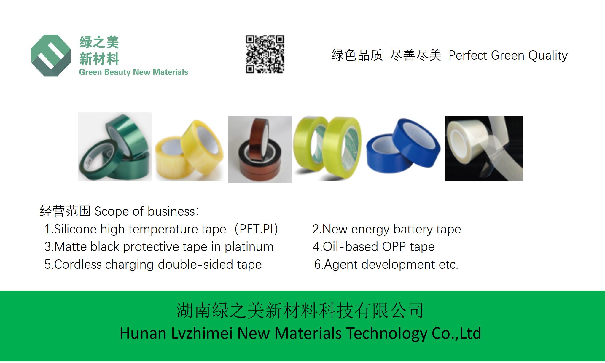
Hunan Lvzhimei New Material Technology Co., Ltd.
Quick Links
Product Categories
© 2024 Hunan Lvzhimei New Material Technology Co., Ltd.All Rights Reserved. Designed by Erge
0731 - 89717319
hnlzm@lvmeikapton.com
+86 13787123465
Room 502, Chuangye Building, No186, Guyuan Road, High-Tech District, Changsha, Hunan, China
CONTACT


